

What Happens When You Write A Bit To A Register
Affiliate 6: Parallel I/O ports
Jonathan Valvano and Ramesh Yerraballi
The chapter covers the purpose of parallel ports, how to programme them using memory-mapped I/O and initialization rituals. We will learn how to access I/O registers in a friendly manner. We will test the system by single-stepping in the simulator, and we will discover the running organization using a logic analyzer.
| Learning Objectives:
|
Video 6.0. Introduction to Parallel Ports, Memory-mapped access and Debugging |
half dozen.0. Introduction
Our offset input/output interfaces volition apply the parallel ports or GPIO, allowing united states to commutation digital information with the external earth. From the very beginning of a project, we must consider how the organisation will be tested. In this chapter we present some debugging techniques that will exist very useful for verifying proper operation of our system. Effective debugging tools are designed into the organisation condign part of the system, rather than attached onto the system afterwards it is built.
In this chapter, we present the I/O pin configurations for the TM4C123 microcontrollers. The regular function of a pin is to perform parallel I/O. Nearly pins, however, have an alternative function. For case, port pins PA1 and PA0 can be either regular parallel port pins or an asynchronous serial port called universal asynchronous receiver/transmitter (UART). The ability to manage time, as an input measurement and an output parameter, has made a pregnant impact on the market share growth of microcontrollers. Articulation Test Action Group (JTAG), standardized as the IEEE 1149.1, is a standard test admission port used to program and debug the microcontroller board. Each microcontroller uses 5 port pins for the JTAG interface.
Common Error: Even though it is possible to utilize the five JTAG pins as general I/O, debugging most microcontroller boards will be more stable if these five pins are left dedicated to the JTAG debugger.
I/O pins on Stellaris and Tiva microcontrollers have a broad range of culling functions:
• UART Universal asynchronous receiver/transmitter
• SSI Synchronous series interface
• IiiC Inter-integrated circuit
• Timer Periodic interrupts, input capture, and output compare
• PWM Pulse width modulation
• ADC Analog to digital converter, measure out analog signals
• Analog Comparator Compar e 2 analog signals
• QEI Quadrature encoder interface
• USB Universal serial autobus
• Ethernet Loftier-speed network
• Can Controller area network
The UART can be used for series communication between computers. Information technology is asynchronous and allows for simultaneous communication in both directions. The SSI is alternately called serial peripheral interface (SPI). It is used to interface medium-speed I/O devices. In this book, nosotros volition employ information technology to interface a graphics display. We could utilise SSI to interface a digital to analog converter (DAC) or a secure digital carte du jour (SDC). IiiC is a simple I/O bus that we will use to interface low speed peripheral devices. Input capture and output compare volition be used to create periodic interrupts and mensurate catamenia, pulse width, phase, and frequency. PWM outputs will exist used to apply variable ability to motor interfaces. In a typical motor controller, input capture measures rotational speed, and PWM controls power. A PWM output can besides exist used to create a DAC. The ADC will exist used to measure the amplitude of analog signals and will exist important in information conquering systems. The analog comparator takes two analog inputs and produces a digital output depending on which analog input is greater. The QEI can be used to interface a brushless DC motor. USB is a high-speed serial communication channel. The Ethernet port can be used to bridge the microcontroller to the Internet or a local area network. The CAN creates a loftier-speed advice channel between microcontrollers and is commonly found in automotive and other distributed command applications.
Ascertainment: The expression mixed-signal refers to a arrangement with both analog and digital components. Notice how many I/O ports perform this analog↔digital bridge: ADC, DAC, analog comparator, PWM, QEI, Input capture, and output compare.
6.1. Stellaris LM4F120 and Tiva TM4C123 LaunchPad I/O pins
Figure vi.1 draws the I/O port structure for the LM4F120H5QR and TM4C123GH6PM . These microcontrollers are used on the EK-LM4F120XL and EK-TM4C123GXL LaunchPads . Pins on the LM3S family accept two possibilities: digital I/O or an alternative function. Still, pins on the LM4F/TM4C family unit can be assigned to as many as eight dissimilar I/O functions. Pins tin be configured for digital I/O, analog input, timer I/O, or series I/O. For example PA0 can be digital I/O or serial input. At that place are 2 buses used for I/O. The digital I/O ports are continued to both the advanced peripheral bus and the advanced high-performance autobus. Because of the multiple buses, the microcontroller tin perform I/O autobus cycles simultaneous with instruction fetches from wink ROM. The LM4F120H5QR has eight UART ports, four SSI ports, four I2C ports, two 12-chip ADCs, twelve timers, a CAN port, and a USB interface. The TM4C123GH6PM adds up to 16 PWM outputs. At that place are 43 I/O lines. There are twelve ADC inputs; each ADC can convert up to 1M samples per second. Table 6.1 lists the regular and alternate names of the port pins.
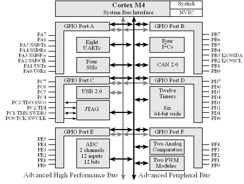
Figure half dozen.1. I/O port pins for the LM4F120H5QR / TM4C123GH6PM microcontrollers.
Each pin has 1 configuration bit in the GPIOAMSEL register. We fix this bit to connect the port pin to the ADC or analog comparator. For digital functions, each pivot also has iv bits in the GPIOPCTL annals, which nosotros ready to specify the alternative part for that pin (0 means regular I/O port). Not every pivot can be connected to every alternative role. See Table 6.1.
Pins PC3 – PC0 were left off Table 6.1 because these four pins are reserved for the JTAG debugger and should not exist used for regular I/O. Notice, near alternate function modules (e.g., U0Rx) merely be on ane pivot (PA0). While other functions could be mapped to 2 or three pins (e.g., CAN0Rx could be mapped to one of the following: PB4, PE4, or PF0.)
For case, if we wished to use UART7 on pins PE0 and PE1, we would set bits 1,0 in the GPIO_PORTE_DEN_R annals (enable digital), clear bits 1,0 in the GPIO_PORTE_AMSEL_R register (disable analog), gear up the PMCx bits in the GPIO_PORTE_PCTL_R register for PE0, PE1 to 0001 (enable UART functionality), and prepare bits 1,0 in the GPIO_PORTE_AFSEL_R register (enable alternate function). If nosotros wished to sample an analog signal on PD0, nosotros would set chip 0 in the alternate part select register, clear scrap 0 in the digital enable register (disable digital), set bit 0 in the analog mode select register (enable analog), and activate one of the ADCs to sample aqueduct 7.
| IO | Ain | 0 | 1 | two | 3 | four | 5 | 6 | 7 | eight | nine | 14 |
| PA0 | Port | U0Rx | CAN1Rx | |||||||||
| PA1 | Port | U0Tx | CAN1Tx | |||||||||
| PA2 | Port | SSI0Clk | ||||||||||
| PA3 | Port | SSI0Fss | ||||||||||
| PA4 | Port | SSI0Rx | ||||||||||
| PA5 | Port | SSI0Tx | ||||||||||
| PA6 | Port | I2C1SCL | M1PWM2 | |||||||||
| PA7 | Port | I2C1SDA | M1PWM3 | |||||||||
| PB0 | Port | U1Rx | T2CCP0 | |||||||||
| PB1 | Port | U1Tx | T2CCP1 | |||||||||
| PB2 | Port | I2C0SCL | T3CCP0 | |||||||||
| PB3 | Port | I2C0SDA | T3CCP1 | |||||||||
| PB4 | Ain10 | Port | SSI2Clk | M0PWM2 | T1CCP0 | CAN0Rx | ||||||
| PB5 | Ain11 | Port | SSI2Fss | M0PWM3 | T1CCP1 | CAN0Tx | ||||||
| PB6 | Port | SSI2Rx | M0PWM0 | T0CCP0 | ||||||||
| PB7 | Port | SSI2Tx | M0PWM1 | T0CCP1 | ||||||||
| PC4 | C1- | Port | U4Rx | U1Rx | M0PWM6 | IDX1 | WT0CCP0 | U1RTS | ||||
| PC5 | C1+ | Port | U4Tx | U1Tx | M0PWM7 | PhA1 | WT0CCP1 | U1CTS | ||||
| PC6 | C0+ | Port | U3Rx | PhB1 | WT1CCP0 | USB0epen | ||||||
| PC7 | C0- | Port | U3Tx | WT1CCP1 | USB0pflt | |||||||
| PD0 | Ain7 | Port | SSI3Clk | SSI1Clk | I2C3SCL | M0PWM6 | M1PWM0 | WT2CCP0 | ||||
| PD1 | Ain6 | Port | SSI3Fss | SSI1Fss | I2C3SDA | M0PWM7 | M1PWM1 | WT2CCP1 | ||||
| PD2 | Ain5 | Port | SSI3Rx | SSI1Rx | M0Fault0 | WT3CCP0 | USB0epen | |||||
| PD3 | Ain4 | Port | SSI3Tx | SSI1Tx | IDX0 | WT3CCP1 | USB0pflt | |||||
| PD4 | USB0DM | Port | U6Rx | WT4CCP0 | ||||||||
| PD5 | USB0DP | Port | U6Tx | WT4CCP1 | ||||||||
| PD6 | Port | U2Rx | M0Fault0 | PhA0 | WT5CCP0 | |||||||
| PD7 | Port | U2Tx | PhB0 | WT5CCP1 | NMI | |||||||
| PE0 | Ain3 | Port | U7Rx | |||||||||
| PE1 | Ain2 | Port | U7Tx | |||||||||
| PE2 | Ain1 | Port | ||||||||||
| PE3 | Ain0 | Port | ||||||||||
| PE4 | Ain9 | Port | U5Rx | I2C2SCL | M0PWM4 | M1PWM2 | CAN0Rx | |||||
| PE5 | Ain8 | Port | U5Tx | I2C2SDA | M0PWM5 | M1PWM3 | CAN0Tx | |||||
| PF0 | Port | U1RTS | SSI1Rx | CAN0Rx | M1PWM4 | PhA0 | T0CCP0 | NMI | C0o | |||
| PF1 | Port | U1CTS | SSI1Tx | M1PWM5 | PhB0 | T0CCP1 | C1o | TRD1 | ||||
| PF2 | Port | SSI1Clk | M0Fault0 | M1PWM6 | T1CCP0 | TRD0 | ||||||
| PF3 | Port | SSI1Fss | CAN0Tx | M1PWM7 | T1CCP1 | TRCLK | ||||||
| PF4 | Port | M1Fault0 | IDX0 | T2CCP0 | USB0epen |
Table half dozen.1. PMCx bits in the GPIOPCTL register on the LM4F/TM4C specify alternate functions. PD4 and PD5 are hardwired to the USB device. PA0 and PA1 are hardwired to the serial port. PWM non on LM4F120.
The LaunchPad evaluation board (Effigy half-dozen.ii) is a low-cost development board available as part number EK-LM4F120XL and EK-TM4C123GXL from https://estore.ti.com/ and in the US from regular electronic distributors like Digikey, Mouser, Arrow, Newark, and Avnet. For detailed instruction for obtaining the lab kit, refer to http://users.ece.utexas.edu/~valvano/edX/. The microcontroller lath provides an integrated In-Circuit Debug Interface (ICDI), which allows programming and debugging of the onboard LM4F120 or TM4C123 microcontroller. Ane USB cable is used by the debugger (ICDI), and the other USB allows the user to develop USB applications (device). The user can select lath power to come from either the debugger (ICDI) or the USB device (device) by setting the Power selection switch.
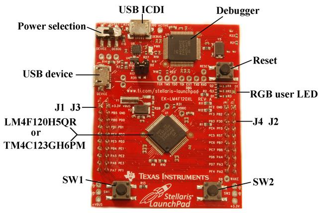
Effigy half dozen.2. Tiva LaunchPad based on the LM4F120H5QR or TM4C123GH6PM.
Pins PA1 – PA0 create a serial port, which is linked through the debugger cablevision to the PC. The serial link is a physical UART equally seen past the LF4F120/TM4C and mapped to a virtual COM port on the PC. The USB device interface uses PD4 and PD5. The JTAG debugger requires pins PC3 – PC0. The LaunchPad connects PB6 to PD0, and PB7 to PD1. If you wish to utilise both PB6 and PD0 you will need to remove the R9 resistor. Similarly, to use both PB7 and PD1 remove the R10 resistor.
The Tiva LaunchPad evaluation board has two switches and ane 3-color LED. Run into Figure 6.3. The switches are negative logic and will require activation of the internal pull-upwardly resistors. In particular, you lot volition fix bits 0 and iv in GPIO_PORTF_PUR_R register. The LED interfaces on PF3 – PF1 are positive logic. To employ the LED, make the PF3 – PF1 pins an output. To activate the red color, output a one to PF1. The bluish color is on PF2, and the dark-green color is controlled by PF3. The 0-Ω resistors (R1, R2, R11, R12, R13, R25, and R29) tin be removed to disconnect the corresponding pin from the external hardware.
The LaunchPad has four ten-pin connectors, labeled every bit J1 J2 J3 J4 in Figures 6.2 and vi.4, to which y'all can adhere your external signals. The summit side of these connectors has male pins, and the bottom side has female sockets. The intent is to stack boards together to brand a layered system. Texas Instruments besides supplies Booster Packs, which are pre-made external devices that will plug into this 40-pin connector. The Booster Packs for the MSP430 LaunchPad are compatible with this board. One simply plugs the 20-pin connectors of the MSP430 booster into the outer two rows. The inner x-pin headers (connectors J3 and J4) use only to Stellaris or Tiva Booster Packs.
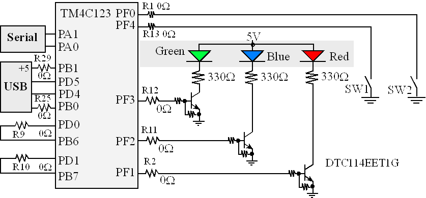
Figure 6.3. Switch and LED interfaces on the Tiva LaunchPad Evaluation Board. The nada ohm resistors can be removed so the corresponding pin tin can be used for its regular purpose.
There are a number of good methods to connect external circuits to the LaunchPad. One method is to purchase a male person to female jumper cable (e.g., item number 826 at www.adafruit.com). A second method is to solder a solid wire into a female socket (east.g., Hirose DF11-2428SCA) creating a male person to female jumper wire.
Since the LaunchPad has both male and female person headers, a very inexpensive method to build systems is to connect solid 24 gauge wire to the female headers on the bottom.
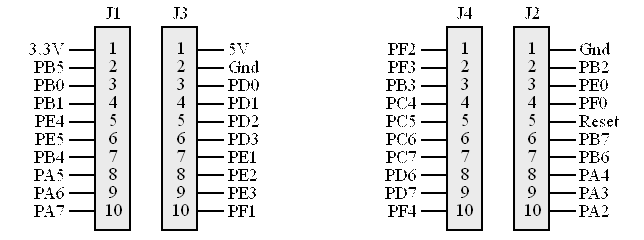
Effigy 6.iv. Interface connectors on the Tiva LM4F120/TM4C123 LaunchPad Evaluation Board.
Each pin has i configuration bit in the GPIOAMSEL register. Nosotros set this scrap to connect the port pin to the ADC or analog comparator. For digital functions, each pin also has four $.25 in the GPIOPCTL annals, which we set to specify the culling function for that pin (0 means regular I/O port). Not every pin can be connected to every alternative office. Run across Table 6.1.
|
Video 6.1. Overview of Ports |
Video half dozen.2. Launchpad running starter code out of the box |
half dozen.ii. Bones Concepts of Input and Output Ports
The simplest I/O port on a microcontroller is the parallel port. A parallel I/O port is a simple mechanism that allows the software to interact with external devices. It is chosen parallel considering multiple signals can be accessed all at once. An input port, which allows the software to read external digital signals, is read but. That ways a read wheel access from the port accost returns the values existing on the inputs at that time. In item, the tristate driver (triangle shaped circuit in Figure vi.5) volition drive the input signals onto the data double-decker during a read cycle from the port accost. A write cycle admission to an input port usually produces no issue. The digital values existing on the input pins are copied into the microcontroller when the software executes a read from the port accost. There are no digital input-merely ports on the LM4F/TM4C family of microcontrollers. The LM4F/TM4C family of microcontrollers has 5V-tolerant digital inputs, significant an input loftier signal can exist any voltage from two.0 to five.0 V. On the STMicroelectronics STM32F10xx family unit, some inputs are 5-Five tolerant and others are not.

Effigy six.5. A read only input port allows the software to sense external digital signals.
: What happens if the software writes to an input port similar Figure vi.v?
While an input device ordinarily just involves the software reading the port, an output port can participate in both the read and write cycles very much like a regular memory. Figure 6.6 describes a readable output port. A write cycle to the port address will touch the values on the output pins. In particular, the microcontroller places information on the information bus and that data is clocked into the D flip-flops. Since it is a readable output, a read cycle access from the port accost returns the current values existing on the port pins. There are no output-just ports on the LM4F/TM4C family unit of microcontrollers.
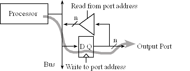
Figure six.6. A readable output port allows the software to generate external digital signals.
: What happens if the software reads from an output port like Figure six.vi?
To make the microcontroller more than marketable, near ports tin be software-specified to be either inputs or outputs. Microcontrollers use the concept of a direction register to make up one's mind whether a pivot is an input (direction register bit is 0) or an output (direction annals bit is i), as shown in Figure 6.seven. We ascertain an initialization ritual every bit a plan executed during outset upwards that initializes hardware and software. If the ritual software makes management flake zero, the port behaves like a simple input, and if it makes the management bit one, it becomes a readable output port. Each digital port pin has a direction chip. This means some pins on a port may be inputs while others are outputs. The digital port pins on near microcontrollers are bidirectional, operating like to Figure 6.7.
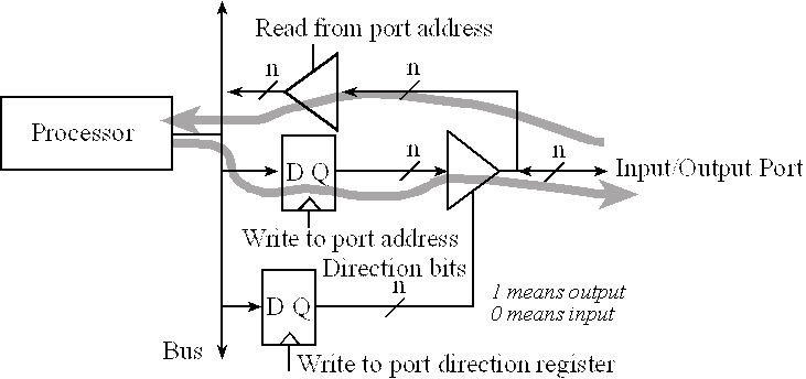
Figure 6.7. A bidirectional port tin be configured as a read-only input port or a readable output port.
Common Error: Many program errors can be traced to defoliation between I/O ports and regular retention. For example, you should not write to an input port, and sometimes we cannot read from an output port.
6.3. I/O Programming and the Direction Annals
On virtually embedded microcontrollers, the I/O ports are memory mapped. This means the software can admission an input/output port simply past reading from or writing to the appropriate accost. Information technology is important to realize that fifty-fifty though I/O operations "look" similar reads and writes to retentiveness variables, the I/O ports often Practice Not act similar memory. For example, some bits are read-but, some are write-but, some can only be cleared, others can only be ready, and some $.25 cannot be modified. To make our software more readable nosotros include symbolic definitions for the I/O ports. Nosotros set up the direction register (eastward.k., GPIO_PORTF_DIR_R ) to specify which pins are input and which are output. Individual port pins can be general purpose I/O (GPIO) or have an alternate function. Nosotros volition set bits in the alternate function annals (e.g., GPIO_PORTF_AFSEL_R ) when nosotros wish to activate the alternate functions listed in Table 6.1. For each I/O pivot we wish to use whether GPIO or alternate office we must enable the digital circuits by setting the bit in the enable register (due east.g., GPIO_PORTF_DEN_R ). Typically, we write to the direction and alternate part registers once during the initialization phase. Nosotros use the data annals (e.grand., GPIO_PORTF_DATA_R ) to perform input/output on the port. Conversely, nosotros read and write the data register multiple times to perform input and output respectively during the running stage. Table six.ii shows some of the parallel port registers for the LM4F120/TM4C123. The just differences amidst the Stellaris and Tiva families are the number of ports and available pins in each port.
| Address | vii | half dozen | 5 | four | three | 2 | 1 | 0 | Name |
| $400F.E608 | -- | -- | GPIOF | GPIOE | GPIOD | GPIOC | GPIOB | GPIOA | SYSCTL_RCGCGPIO_R |
| $4000.43FC | Data | Information | Information | Data | DATA | DATA | DATA | DATA | GPIO_PORTA_DATA_R |
| $4000.4400 | DIR | DIR | DIR | DIR | DIR | DIR | DIR | DIR | GPIO_PORTA_DIR_R |
| $4000.4420 | SEL | SEL | SEL | SEL | SEL | SEL | SEL | SEL | GPIO_PORTA_AFSEL_R |
| $4000.4510 | PUE | PUE | PUE | PUE | PUE | PUE | PUE | PUE | GPIO_PORTA_PUR_R |
| $4000.451C | DEN | DEN | DEN | DEN | DEN | DEN | DEN | DEN | GPIO_PORTA_DEN_R |
| $4000.4524 | 1 | 1 | 1 | 1 | i | 1 | 1 | 1 | GPIO_PORTA_CR_R |
| $4000.4528 | 0 | 0 | 0 | 0 | 0 | 0 | 0 | 0 | GPIO_PORTA_AMSEL_R |
| $4000.53FC | DATA | DATA | DATA | Data | Data | Data | Data | DATA | GPIO_PORTB_DATA_R |
| $4000.5400 | DIR | DIR | DIR | DIR | DIR | DIR | DIR | DIR | GPIO_PORTB_DIR_R |
| $4000.5420 | SEL | SEL | SEL | SEL | SEL | SEL | SEL | SEL | GPIO_PORTB_AFSEL_R |
| $4000.5510 | PUE | PUE | PUE | PUE | PUE | PUE | PUE | PUE | GPIO_PORTB_PUR_R |
| $4000.551C | DEN | DEN | DEN | DEN | DEN | DEN | DEN | DEN | GPIO_PORTB_DEN_R |
| $4000.5524 | 1 | 1 | 1 | one | 1 | 1 | 1 | ane | GPIO_PORTB_CR_R |
| $4000.5528 | 0 | 0 | AMSEL | AMSEL | 0 | 0 | 0 | 0 | GPIO_PORTB_AMSEL_R |
| $4000.63FC | DATA | DATA | Data | DATA | JTAG | JTAG | JTAG | JTAG | GPIO_PORTC_DATA_R |
| $4000.6400 | DIR | DIR | DIR | DIR | JTAG | JTAG | JTAG | JTAG | GPIO_PORTC_DIR_R |
| $4000.6420 | SEL | SEL | SEL | SEL | JTAG | JTAG | JTAG | JTAG | GPIO_PORTC_AFSEL_R |
| $4000.6510 | PUE | PUE | PUE | PUE | JTAG | JTAG | JTAG | JTAG | GPIO_PORTC_PUR_R |
| $4000.651C | DEN | DEN | DEN | DEN | JTAG | JTAG | JTAG | JTAG | GPIO_PORTC_DEN_R |
| $4000.6524 | 1 | 1 | 1 | 1 | JTAG | JTAG | JTAG | JTAG | GPIO_PORTC_CR_R |
| $4000.6528 | AMSEL | AMSEL | AMSEL | AMSEL | JTAG | JTAG | JTAG | JTAG | GPIO_PORTC_AMSEL_R |
| $4000.73FC | DATA | DATA | DATA | DATA | DATA | DATA | Information | Information | GPIO_PORTD_DATA_R |
| $4000.7400 | DIR | DIR | DIR | DIR | DIR | DIR | DIR | DIR | GPIO_PORTD_DIR_R |
| $4000.7420 | SEL | SEL | SEL | SEL | SEL | SEL | SEL | SEL | GPIO_PORTD_AFSEL_R |
| $4000.7510 | PUE | PUE | PUE | PUE | PUE | PUE | PUE | PUE | GPIO_PORTD_PUR_R |
| $4000.751C | DEN | DEN | DEN | DEN | DEN | DEN | DEN | DEN | GPIO_PORTD_DEN_R |
| $4000.7524 | CR | 1 | one | ane | 1 | i | 1 | one | GPIO_PORTD_CR_R |
| $4000.7528 | 0 | 0 | AMSEL | AMSEL | AMSEL | AMSEL | AMSEL | AMSEL | GPIO_PORTD_AMSEL_R |
| $4002.43FC | DATA | Data | Information | Data | DATA | Data | GPIO_PORTE_DATA_R | ||
| $4002.4400 | DIR | DIR | DIR | DIR | DIR | DIR | GPIO_PORTE_DIR_R | ||
| $4002.4420 | SEL | SEL | SEL | SEL | SEL | SEL | GPIO_PORTE_AFSEL_R | ||
| $4002.4510 | PUE | PUE | PUE | PUE | PUE | PUE | GPIO_PORTE_PUR_R | ||
| $4002.451C | DEN | DEN | DEN | DEN | DEN | DEN | GPIO_PORTE_DEN_R | ||
| $4002.4524 | 1 | 1 | one | i | 1 | 1 | GPIO_PORTE_CR_R | ||
| $4002.4528 | AMSEL | AMSEL | AMSEL | AMSEL | AMSEL | AMSEL | GPIO_PORTE_AMSEL_R | ||
| $4002.53FC | DATA | DATA | Information | Data | Data | GPIO_PORTF_DATA_R | |||
| $4002.5400 | DIR | DIR | DIR | DIR | DIR | GPIO_PORTF_DIR_R | |||
| $4002.5420 | SEL | SEL | SEL | SEL | SEL | GPIO_PORTF_AFSEL_R | |||
| $4002.5510 | PUE | PUE | PUE | PUE | PUE | GPIO_PORTF_PUR_R | |||
| $4002.551C | DEN | DEN | DEN | DEN | DEN | GPIO_PORTF_DEN_R | |||
| $4002.5524 | 1 | 1 | 1 | 1 | CR | GPIO_PORTF_CR_R | |||
| $4002.5528 | 0 | 0 | 0 | 0 | 0 | GPIO_PORTF_AMSEL_R | |||
| 31-28 | 27-24 | 23-xx | 19-16 | 15-12 | 11-8 | 7-4 | 3-0 | ||
| $4000.452C | PMC7 | PMC6 | PMC5 | PMC4 | PMC3 | PMC2 | PMC1 | PMC0 | GPIO_PORTA_PCTL_R |
| $4000.552C | PMC7 | PMC6 | PMC5 | PMC4 | PMC3 | PMC2 | PMC1 | PMC0 | GPIO_PORTB_PCTL_R |
| $4000.652C | PMC7 | PMC6 | PMC5 | PMC4 | 0x1 | 0x1 | 0x1 | 0x1 | GPIO_PORTC_PCTL_R |
| $4000.752C | PMC7 | PMC6 | PMC5 | PMC4 | PMC3 | PMC2 | PMC1 | PMC0 | GPIO_PORTD_PCTL_R |
| $4002.452C | PMC5 | PMC4 | PMC3 | PMC2 | PMC1 | PMC0 | GPIO_PORTE_PCTL_R | ||
| $4002.552C | PMC4 | PMC3 | PMC2 | PMC1 | PMC0 | GPIO_PORTF_PCTL_R | |||
| $4000.6520 | LOCK (write 0x4C4F434B to unlock, other locks) (reads 1 if locked, 0 if unlocked) | GPIO_PORTC_LOCK_R | |||||||
| $4000.7520 | LOCK (write 0x4C4F434B to unlock, other locks) (reads 1 if locked, 0 if unlocked) | GPIO_PORTD_LOCK_R | |||||||
| $4002.5520 | LOCK (write 0x4C4F434B to unlock, other locks) (reads one if locked, 0 if unlocked) | GPIO_PORTF_LOCK_R | |||||||
Table 6.2 Some TM4C123 parallel ports. Each annals is 32 bits wide. For PMCx bits, see Table 6.i. JTAG means practise not use these pins and do not change any of these $.25.
To initialize an I/O port for general apply nosotros perform seven steps. Steps two through iv are needed only for the LM4F/TM4C microcontrollers. Outset, nosotros activate the clock for the port. Second, we unlock the port; unlocking is needed only for pins PC3-0, PD7, PF0 on the LM4F and TM4C. Third, we disable the analog function of the pin, because we volition exist using the pin for digital I/O. Fourth, nosotros clear bits in the PCTL (Table 6.1) to select regular digital function. 5th, we set its direction annals. 6th, we clear bits in the alternating function register, and lastly, nosotros enable the digital port. We need to add a curt delay between activating the clock and accessing the port registers. The direction annals specifies bit for chip whether the respective pins are input or output. A DIR scrap of 0 means input and 1 means output.
Mutual Fault: You will go a bus fault if yous admission a port without enabling its clock.
In this outset example we volition make PF4 and PF0 input, and nosotros volition brand PF3 PF2 and PF1 output, as shown in Program 6.1. To use a port we start must activate its clock in the SYSCTL_RCGCGPIO_R register. The second step is to unlock the port, past writing a special value to the LOCK register, followed by setting bits in the CR annals. Just PC3-0, PD7, and PF0 on the TM4C need to be unlocked. All the other $.25 on the TM4C are always unlocked. The third pace is to disable the analog functionality, by clearing bits in the AMSEL register. The quaternary step is to select GPIO functionality, by clearing bits in the PCTL register, as described in Tabular array 6.1. The fifth step is to specify whether the pin is an input or an output past clearing or setting bits in the DIR annals. Because we are using the pins as regular digital I/O, the 6th pace is to clear the corresponding bits in the AFSEL register. The last step is to enable the corresponding I/O pins past writing ones to the DEN register. To run this case on the LaunchPad, we besides set bits in the PUR register for the two switch inputs (Figure 6.iii) to take an internal pull-upwards resistor.
When the software reads from location 0x400253FC, the bottom 8 bits are returned with the current values on Port F. The tiptop 24 bits are returned nil. Equally shown in Figure 6.vii, when reading an I/O port, the input pins show the electric current digital state, and the output pins show the value last written to the port. The part PortF_Input will read from the five input pins, and return a value depending on the current status of the inputs. As shown in Effigy half-dozen.7, when writing to an I/O port, the input pins are not affected, and the output pins are changed to the value written to the port. The part PortF_Output will write new values to the 3 output pins. The #include will define symbolic names for all the I/O ports for that microcontroller. The header file tm4c123ge6pm.h tin can be found in the inc folder.
#include "tm4c123ge6pm.h"
unsigned long In; // input from PF4
unsigned long Out; // output to PF2 (blue LED)
// Part Prototypes
void PortF_Init(void);
// 3. Subroutines Section
// MAIN: Mandatory for a C Program to be executable
int main(void){ // initialize PF0 and PF4 and make them inputs
PortF_Init(); // make PF3-1 out (PF3-1 built-in LEDs)
while(1){
In = GPIO_PORTF_DATA_R&0x10; // read PF4 into Sw1
In = In>>2; // shift into position PF2
Out = GPIO_PORTF_DATA_R;
Out = Out&0xFB;
Out = Out|In;
GPIO_PORTF_DATA_R = Out; // output
}
}
// Subroutine to initialize port F pins for input and output
// PF4 is input SW1 and PF2 is output Blue LED
// Inputs: None
// Outputs: None
// Notes: ...
void PortF_Init(void){ volatile unsigned long delay;
SYSCTL_RCGCGPIO_R |= 0x00000020; // 1) activate clock for Port F
delay = SYSCTL_RCGCGPIO_R; // allow fourth dimension for clock to start
GPIO_PORTF_LOCK_R = 0x4C4F434B; // ii) unlock GPIO Port F
GPIO_PORTF_CR_R = 0x1F; // permit changes to PF4-0
// merely PF0 needs to be unlocked, other bits can't exist locked
GPIO_PORTF_AMSEL_R = 0x00; // iii) disable analog on PF
GPIO_PORTF_PCTL_R = 0x00000000; // 4) PCTL GPIO on PF4-0
GPIO_PORTF_DIR_R = 0x0E; // 5) PF4,PF0 in, PF3-ane out
GPIO_PORTF_AFSEL_R = 0x00; // 6) disable alt funct on PF7-0
GPIO_PORTF_PUR_R = 0x11; // enable pull-upward on PF0 and PF4
GPIO_PORTF_DEN_R = 0x1F; // seven) enable digital I/O on PF4-0
}
Programme 6.1. A set of functions using PF4,PF0 as inputs and PF3-one as outputs (C6_InputOutputxxx.naught).
: Does the entire port need to be defined every bit input or output, or can some pins be input while others are output?
: How do we change Plan vi.1 to run using Port A?
Interactive Tool vi.1
The following tool allows you to test your understanding of what happens when you lot WRITE to the Data register for PortF.
Annotation, writing to input pins has no effect. See what happens if you click on one of the 2 switches.
Enter a 5 flake number to write to GPIO_PORTF_DATA_R, bits iv through 0:
Video 6.3. Device registers, Port Initialization steps with an PortF every bit an instance
In Program 6.i the supposition was the software module had access to all of Port F. In other words, this software owned all pins of Port F. In near cases, a software module needs access to only some of the port pins. If ii or more software modules access the aforementioned port, a conflict will occur if i module changes modes or output values set past another module. Information technology is good software design to write friendly software, which only affects the individual pins as needed. Friendly software does not modify the other $.25 in a shared register. Conversely, unfriendly software modifies more than bits of a annals than it needs to. The difficulty of unfriendly code is each module will run properly when tested by itself, merely weird bugs result when 2 or more modules are combined.
Consider the problem that a software module needs to output to only Port A chip 7. Afterwards enabling the clock for Port A, we use read-modify-write software to initialize simply pin 7. The following initialization does not modify the configurations for the other seven bits in Port A. Unlocking is not required for PA7 (just PD7 and PF0 require unlocking)
SYSCTL_RCGCGPIO_R |= 0x00000001; // 1) actuate clock for Port A
delay = SYSCTL_RCGCGPIO_R; // allow time for clock to offset
GPIO_PORTA_AMSEL_R &= ~0x80; // 3) disable analog on PA7
GPIO_PORTA_PCTL_R &= ~0xF0000000; // 4) PCTL GPIO on PA7
GPIO_PORTA_DIR_R |= 0x80; // 5) PA7 out
GPIO_PORTA_AFSEL_R &= ~0x80; // 6) disable alt funct on PA7
GPIO_PORTA_DEN_R |= 0x80; // 7) enable digital I/O on PA7
In that location is no disharmonize if two or more modules enable the clock for Port A. There are two ways on LM4F/TM4C microcontrollers to admission individual port bits. The first method is to use read-modify-write software to change merely one pin. A read-or-write sequence can be used to set $.25.
| LDR R1, =GPIO_PORTA_DATA_R LDR R0, [R1] ; previous ORR R0, R0, #0x80 ; set bit 1 STR R0, [R1] | // brand PA7 high GPIO_PORTA_DATA_R |= 0x80; |
A read-and-write sequence can be used to clear one or more than bits.
| LDR R1, =GPIO_PORTA_DATA_R LDR R0, [R1] ; previous BIC R0, R0, #0x80 ; clear bit 1 STR R0, [R1] | // brand PA7 low GPIO_PORTA_DATA_R &= ~0x80; |
|
Video 6.v. Software Evolution of solution |
Video 6.6. Writing friendly code |
The second method uses the bit-specific addressing. The LM4F/TM4C family implements a flexible way to access port pins. This flake-specific addressing doesn't work for all the I/O registers, merely the parallel port information registers. The machinery allows collective admission to 1 to viii bits in a data port. Nosotros define viii address offset constants in Table vi.iii. Basically, if we are interested in scrap b, the constant is iv*2 b . There 256 possible bit combinations nosotros might exist interested in accessing, from all of them to none of them. Each possible bit combination has a carve up address for accessing that combination. For each fleck we are interested in, nosotros add up the corresponding constants from Table 6.iii and then add that sum to the base address for the port. The base of operations addresses for the information ports can exist found Table half dozen.2. For case, assume we are interested in Port A bits 1, two, and 3. The base address for Port A is 0x4000.4000, and the constants are 0x0008, 0x0010, and 0x0020. The sum of 0x4000.4000+0x0008+0x0010 +0x0020 is the address 0x4000.4038. If we read from 0x4000.4038 only $.25 1, 2, and iii will be returned. If nosotros write to this address only $.25 ane, 2, and 3 volition be modified.
| If nosotros wish to access bit | Constant |
| 7 | 0x0200 |
| 6 | 0x0100 |
| 5 | 0x0080 |
| 4 | 0x0040 |
| 3 | 0x0020 |
| 2 | 0x0010 |
| ane | 0x0008 |
| 0 | 0x0004 |
Table 6.3. Accost offsets used to specify individual data port $.25.
The base address for Port A is 0x4000.4000. If nosotros want to read and write all 8 bits of this port, the constants will add up to 0x03FC. Notice that the sum of the base accost and the constants yields the 0x4000.43FC accost used in Table 6.2 and Program half-dozen.1. In other words, read and write operations to GPIO_PORTA_DATA_R volition admission all 8 bits of Port A. If we are interested in just bit five of Port A, nosotros add 0x0080 to 0x4000.4000, and we tin define this in C and in assembly as
#define PA5 (*((volatile unsigned long *)0x40004080))
PA5 EQU 0x40004080
Now, a simple write operation tin can be used to prepare PA5. The following code is friendly considering it does not modify the other vii bits of Port A.
PA5 = 0x20; // brand PA5 loftier
A simple write sequence will clear PA5. The post-obit code is likewise friendly.
PA5 = 0x00; // make PA5 low
A read from PA5 volition return 0x20 or 0x00 depending on whether the pin is high or low, respectively. If PA5 is an output, the post-obit lawmaking is also friendly.
PA5 = PA5^0x20; // toggle PA5
Note that the base address when calculating the flake-specific accost for PortA is 0x40004000, the following tabular array lists the base of operations addresses for the other ports.
| Port | Base address |
|---|---|
| PortA | 0x40004000 |
| PortB | 0x40005000 |
| PortC | 0x40006000 |
| PortD | 0x40007000 |
| PortE | 0x40024000 |
| PortF | 0x40025000 |
Table 6.iv. Base Addresses for bit-specific addressing of ports A-F
: What happens if we write to location 0x4000.4000?
: Specify a #define that allows us to admission $.25 seven and 1 of Port A. Employ this #define to brand both $.25 7 and 1 of Port A high.
: Specify a #define that allows us to access bits 6, 1, 0 of Port B. Utilize this #ascertain to brand $.25 6, 1 and 0 of Port B high.
To understand the port definitions in C, we remember #define is simply a re-create paste. East.g.,
data = PA5;
becomes
information = (*((volatile unsigned long *)0x40004080)) ;
To empathise why we define ports this way, allow's pause this port definition into pieces. First, 0x40004080 is the address of Port A fleck 5. If we write merely #ascertain PA5 0x40004080 it will create
data = 0x40004080;
which does not read the contents of PA5 as desired. This means we need to dereference the address. If nosotros write #define PA5 (*0x40004080) it will create
data = (*0x40004080);
This will attempt to read the contents at 0x40004080, but doesn't know whether to read 8 16 or 32 bits. So the compiler gives a syntax fault because the type of data does non match the type of (*0x40004080). To solve a type mismatch in C we typecast, placing a (new type) in front of the object we wish to catechumen. We wish force the type conversion to unsigned 32 bits, so we alter the definition to include the typecast,
#define PA5 (*((volatile unsigned long *)0x40004080) )
The volatile is added because the value of a port can change across the direct activeness of the software. Information technology forces the C compiler to read a new value each time through a loop and non rely on the previous value.
6.iv. Debugging monitor using an LED
Ane of the important tasks in debugging a arrangement is to observe when and where our software is executing. A debugging tool that works well for real-time systems is the monitor. In a real-time organization, nosotros demand the execution time of the debugging tool to exist small compared to the execution time of the program itself. Intrusiveness is defined as the degree to which the debugging code itself alters the performance of the system beingness tested. A monitor is an independent output process, somewhat similar to the impress statement, just ane that executes much faster and thus is much less intrusive. An LED fastened to an output port of the microcontroller is an example of a BOOLEAN monitor. You lot tin place LEDs on unused output pins. Software toggles these LEDs to let you lot know where and when your program is running. Presume an LED is attached to Port F bit two. Plan six.two will toggle the LED. We create a flake-specific address constant to access but PF2:
| PF2 EQU 0x40025010 Toggle LDR R1, =PF2 LDR R0, [R1] EOR R0, R0, #0x04 STR R0, [R1] BX LR | #ascertain PF2 (*((volatile unsigned long *)0x40025010)) void Toggle(void){ PF2 ^= 0x04; // toggle LED } |
Programme 6.2. An LED monitor.
A heartbeat is a pulsing output that is not required for the correct operation of the system, but it is useful to see while the program is running. In particular, you add BL Toggle statements at strategic places inside your organisation. It only takes 13 bus cycles to execute. Port G must be initialized and then that bit two is an output before the debugging begins. You can either discover the LED directly or look at the LED control signals with a loftier-speed oscilloscope or logic analyzer. An LCD tin be an effective monitor for small amounts of information. Inexpensive LCDs can display from 8 to 160 characters. Unfortunately, it takes about 50 µs to output each character, so the utilize of an LCD monitor might be intrusive. When using LED monitors it is better to modify just the i scrap, leaving the other 7 as is. In this way, y'all can have additional LED monitors.
vi.five. Hardware debugging tools
Microcomputer related problems often require the apply of specialized equipment to debug the system hardware and software. Two very useful tools are the logic analyzer and the oscilloscope. A logic analyzer is essentially a multiple aqueduct digital storage scope with many means to trigger, meet Figure 6.8. As a troubleshooting aid, it allows the experimenter to observe numerous digital signals at diverse points in time and thus make decisions based upon such observations. Equally with whatever debugging process, it is necessary to select which information to observe out of a vast set of possibilities. Whatever digital indicate in the system can be continued to the logic analyzer. Effigy 6.8 shows an eight-aqueduct logic analyzer, merely existent devices tin support 128 or more channels. One problem with logic analyzers is the massive amount of information that it generates. With logic analyzers (similar to other debugging techniques) we must strategically select which signals in the digital interfaces to observe and when to find them. In item, the triggering machinery can be used to capture information at appropriate times eliminating the need to sift through volumes of output. Sometimes there are extra I/O pins on the microcontroller, not needed for the normal operation of the system (shown equally the bottom two wires in Figure 6.8). In this case, we can connect the pins to a logic analyzer, and add together software debugging instruments that set and articulate these pins at strategic times inside the software. In this way we can visualize the hardware/software timing.
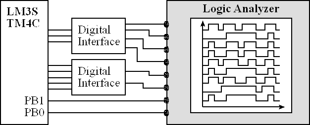
Figure 6.eight. A logic analyzer and example output.
An oscilloscope tin can be used to capture voltage versus time data. You lot can arrange the voltage range and time scale. The oscilloscope trigger is how and when the data will exist capture. In normal mode, we measure patterns that repeat over and over, and we use the trigger (eastward.m., rising border of channel 1) to freeze the image. In single shot manner, the display is initially blank, and once the trigger occurs, one trace is captured and brandish.
vi.6. Chapter 6 Quiz
6.one To make a pin a digital input, what value do you load into corresponding $.25 the post-obit registers. Assume it does not demand an internal pullup
                                          DIR
                PUR
  PCTL
                AFSEL
                AMSEL
                DEN
6.2 To brand a pin a digital output, what value do you load into corresponding bits the following registers. Assume it does not demand an internal pullup
                                          DIR
                PUR
  PCTL
                AFSEL
                AMSEL
                DEN
half dozen.3 Which line of C code is a friendly way to set Port B bit 2 assuming this pin has already been initialized as an output
GPIO_PORTB_DATA_R = 0x00;
GPIO_PORTB_DATA_R = 0x02;
GPIO_PORTB_DATA_R = 0x04;
GPIO_PORTB_DATA_R |= 0x02;
GPIO_PORTB_DATA_R |= 0x04;
GPIO_PORTB_DATA_R &= 0x02;
GPIO_PORTB_DATA_R &= 0x04;
GPIO_PORTB_DATA_R &= ~0x02;
GPIO_PORTB_DATA_R &= ~0x04;
six.4 Which line of C lawmaking is a friendly way to articulate Port B scrap 2 assuming this pin has already been initialized as an output
GPIO_PORTB_DATA_R = 0x00;
GPIO_PORTB_DATA_R = 0x02;
GPIO_PORTB_DATA_R = 0x04;
GPIO_PORTB_DATA_R |= 0x02;
GPIO_PORTB_DATA_R |= 0x04;
GPIO_PORTB_DATA_R &= 0x02;
GPIO_PORTB_DATA_R &= 0x04;
GPIO_PORTB_DATA_R &= ~0x02;
GPIO_PORTB_DATA_R &= ~0x04;
6.v Which debugging instrument can measure voltage versus time?
Eye beat
Oscilloscope
Logic analyzer
LED
half-dozen.6 Which debugging instrument tin measure multiple digital signals versus fourth dimension?
Heart beat
Oscilloscope
Logic analyzer
LED
Reprinted with approval from Embedded Systems: Introduction to ARM Cortex-Yard Microcontrollers, 2014, ISBN: 978-1477508992, http://users.ece.utexas.edu/~valvano/arm/outline1.htm

What Happens When You Write A Bit To A Register,
Source: https://users.ece.utexas.edu/~valvano/Volume1/E-Book/C6_MicrocontrollerPorts.htm
Posted by: beattiehouseenjut.blogspot.com
0 Response to "What Happens When You Write A Bit To A Register"
Post a Comment