

How Does A Shift Register Get Bits
Digital Circuits - Shift Registers
We know that one flip-flop can store one-scrap of information. In social club to store multiple bits of information, we crave multiple flip-flops. The group of flip-flops, which are used to agree (store) the binary information is known every bit register.
If the annals is capable of shifting bits either towards right paw side or towards left hand side is known every bit shift annals. An 'Due north' bit shift register contains 'North' flip-flops. Following are the four types of shift registers based on applying inputs and accessing of outputs.
- Serial In − Serial Out shift register
- Serial In − Parallel Out shift annals
- Parallel In − Serial Out shift annals
- Parallel In − Parallel Out shift register
Series In − Serial Out (SISO) Shift Register
The shift annals, which allows serial input and produces serial output is known as Serial In – Series Out (SISO) shift register. The block diagram of 3-scrap SISO shift register is shown in the following figure.
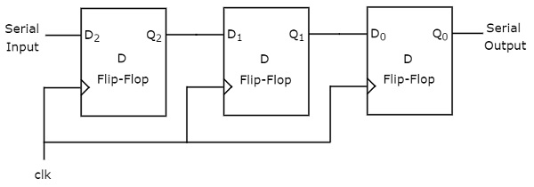
This block diagram consists of three D flip-flops, which are cascaded. That means, output of ane D flip-bomb is continued as the input of next D flip-flop. All these flip-flops are synchronous with each other since, the aforementioned clock signal is practical to each 1.
In this shift register, nosotros can send the $.25 serially from the input of left most D flip-flop. Hence, this input is also chosen as serial input. For every positive edge triggering of clock signal, the data shifts from i phase to the adjacent. And then, we can receive the bits serially from the output of correct nigh D flip-bomb. Hence, this output is as well called as serial output.
Case
Let us see the working of 3-fleck SISO shift register by sending the binary information "011" from LSB to MSB serially at the input.
Assume, initial status of the D flip-flops from leftmost to rightmost is $Q_{ii}Q_{1}Q_{0}=000$. Nosotros tin empathise the working of 3-scrap SISO shift annals from the post-obit table.
| No of positive edge of Clock | Serial Input | Q2 | Qi | Q0 |
|---|---|---|---|---|
| 0 | - | 0 | 0 | 0 |
| 1 | 1(LSB) | i | 0 | 0 |
| 2 | 1 | one | i | 0 |
| 3 | 0(MSB) | 0 | ane | 1(LSB) |
| iv | - | - | 0 | one |
| 5 | - | - | - | 0(MSB) |
The initial status of the D flip-flops in the absence of clock indicate is $Q_{2}Q_{i}Q_{0}=000$. Here, the serial output is coming from $Q_{0}$. So, the LSB (1) is received at 3rd positive edge of clock and the MSB (0) is received at fiveth positive border of clock.
Therefore, the three-bit SISO shift register requires five clock pulses in order to produce the valid output. Similarly, the N-bit SISO shift register requires 2N-one clock pulses in order to shift 'N' bit information.
Series In - Parallel Out (SIPO) Shift Register
The shift register, which allows series input and produces parallel output is known as Serial In – Parallel Out (SIPO) shift annals. The block diagram of 3-bit SIPO shift register is shown in the following figure.
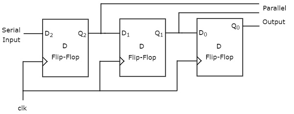
This circuit consists of three D flip-flops, which are cascaded. That ways, output of i D flip-flop is connected as the input of next D flip-bomb. All these flip-flops are synchronous with each other since, the same clock point is applied to each ane.
In this shift register, we can send the bits serially from the input of left about D flip-flop. Hence, this input is too called as serial input. For every positive edge triggering of clock indicate, the data shifts from one stage to the next. In this case, we can admission the outputs of each D flip-flop in parallel. So, we will get parallel outputs from this shift annals.
Case
Let united states of america run into the working of 3-bit SIPO shift register by sending the binary information "011" from LSB to MSB serially at the input.
Assume, initial status of the D flip-flops from leftmost to rightmost is $Q_{two}Q_{ane}Q_{0}=000$. Here, $Q_{two}$ & $Q_{0}$ are MSB & LSB respectively. We can empathize the working of 3-bit SIPO shift register from the following table.
| No of positive edge of Clock | Serial Input | Qtwo(MSB) | Qone | Q0(LSB) |
|---|---|---|---|---|
| 0 | - | 0 | 0 | 0 |
| one | 1(LSB) | i | 0 | 0 |
| 2 | 1 | 1 | 1 | 0 |
| 3 | 0(MSB) | 0 | 1 | 1 |
The initial status of the D flip-flops in the absence of clock signal is $Q_{2}Q_{1}Q_{0}=000$. The binary data "011" is obtained in parallel at the outputs of D flip-flops for third positive edge of clock.
So, the 3-flake SIPO shift register requires iii clock pulses in lodge to produce the valid output. Similarly, the Northward-fleck SIPO shift register requires N clock pulses in order to shift 'North' bit information.
Parallel In − Series Out (PISO) Shift Register
The shift register, which allows parallel input and produces serial output is known as Parallel In − Serial Out (PISO) shift register. The block diagram of iii-bit PISO shift register is shown in the following figure.
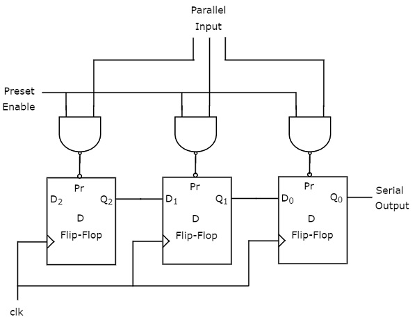
This circuit consists of iii D flip-flops, which are cascaded. That means, output of 1 D flip-flop is connected as the input of next D flip-bomb. All these flip-flops are synchronous with each other since, the same clock signal is applied to each 1.
In this shift register, we can apply the parallel inputs to each D flip-flop by making Preset Enable to i. For every positive edge triggering of clock signal, the information shifts from one stage to the next. So, we volition get the series output from the right most D flip-flop.
Example
Let us run across the working of iii-fleck PISO shift register by applying the binary data "011" in parallel through preset inputs.
Since the preset inputs are applied before positive border of Clock, the initial condition of the D flip-flops from leftmost to rightmost will be $Q_{2}Q_{1}Q_{0}=011$. We can understand the working of three-scrap PISO shift annals from the post-obit table.
| No of positive edge of Clock | Q2 | Q1 | Q0 |
|---|---|---|---|
| 0 | 0 | 1 | 1(LSB) |
| ane | - | 0 | one |
| 2 | - | - | 0(LSB) |
Here, the series output is coming from $Q_{0}$. So, the LSB (1) is received before applying positive edge of clock and the MSB (0) is received at 2nd positive edge of clock.
Therefore, the 3-scrap PISO shift register requires two clock pulses in social club to produce the valid output. Similarly, the Due north-bit PISO shift register requires N-1 clock pulses in society to shift 'North' bit data.
Parallel In - Parallel Out (PIPO) Shift Register
The shift annals, which allows parallel input and produces parallel output is known equally Parallel In − Parallel Out (PIPO) shift register. The block diagram of 3-scrap PIPO shift register is shown in the following figure.
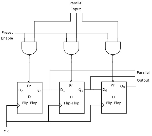
This circuit consists of three D flip-flops, which are cascaded. That ways, output of i D flip-flop is continued as the input of next D flip-flop. All these flip-flops are synchronous with each other since, the aforementioned clock signal is applied to each one.
In this shift register, we can utilize the parallel inputs to each D flip-flop by making Preset Enable to ane. We can apply the parallel inputs through preset or clear. These two are asynchronous inputs. That means, the flip-flops produce the corresponding outputs, based on the values of asynchronous inputs. In this case, the outcome of outputs is independent of clock transition. And so, we will go the parallel outputs from each D flip-flop.
Example
Let united states see the working of three-bit PIPO shift register past applying the binary information "011" in parallel through preset inputs.
Since the preset inputs are applied before positive border of Clock, the initial condition of the D flip-flops from leftmost to rightmost volition be $Q_{two}Q_{1}Q_{0}=011$. So, the binary information "011" is obtained in parallel at the outputs of D flip-flops earlier applying positive border of clock.
Therefore, the 3-scrap PIPO shift register requires zip clock pulses in social club to produce the valid output. Similarly, the N-bit PIPO shift register doesn't require any clock pulse in order to shift 'N' bit information.
Useful Video Courses

Video

Video

Video

Video

Video

Video

How Does A Shift Register Get Bits,
Source: https://www.tutorialspoint.com/digital_circuits/digital_circuits_shift_registers.htm
Posted by: beattiehouseenjut.blogspot.com
0 Response to "How Does A Shift Register Get Bits"
Post a Comment